The BM1366
The BM1366 is an undocumented SHA256 mining ASIC from Bitmain. It’s mostly used in the Antminer S19.
| Price | New: ~$25 Used: ~$15 in small quantities |
| Efficiency | 25J/TH |
| Serial Protocol | UART |
| Baudrate | - |
| Footprint | - |
Pinout
Section titled “Pinout”
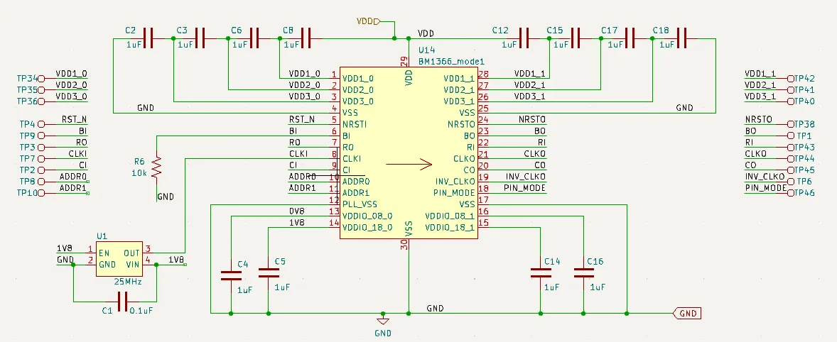
| Pinout | Explanation |
|---|---|
| VDD1_0 | Internal voltage domain 1. (for bypass capacitors) |
| VDD2_0 | Internal voltage domain 2. (for bypass capacitors) |
| VDD3_0 | Internal voltage domain 3. (for bypass capacitors) |
| VSS | Ground |
| NRSTI | Reset input |
| BI | Busy Input |
| RO | Serial Response Output |
| CLKI | Clock Input |
| CI | Serial Command Input |
| ADDR0 | Address 0 (unknown functionality) |
| ADDR1 | Address 1 (unknown functionality) |
| PLL_VSS | Phase Locked Loop Ground |
| VDDIO_08_0 | 0.8V IO voltage |
| VDDIO_18_0 | 1.8V IO voltage (this is normally 1.2V now) |
| VDD1_1 | Internal voltage domain 1. (for bypass capacitors) |
| VDD2_1 | Internal voltage domain 2. (for bypass capacitors) |
| VDD3_1 | Internal voltage domain 3. (for bypass capacitors) |
| VSS | Ground |
| NRST0 | Reset Output |
| BO | Busy Output |
| RI | Serial Response Input |
| CLK0 | Clock output |
| CO | Serial Command Output |
| INV_CLK0 | Inverted Clock Output (unknown use) |
| PIN_MODE | Pin mode selector |
| VSS | Ground |
| VDI0_08_1 | 0.8V IO voltage |
| VSI0_08_1 | 1.8V IO voltage (this is normally 1.2V now) |
Versions
Section titled “Versions”How to identify a cracked “destroyed” chip
Section titled “How to identify a cracked “destroyed” chip”
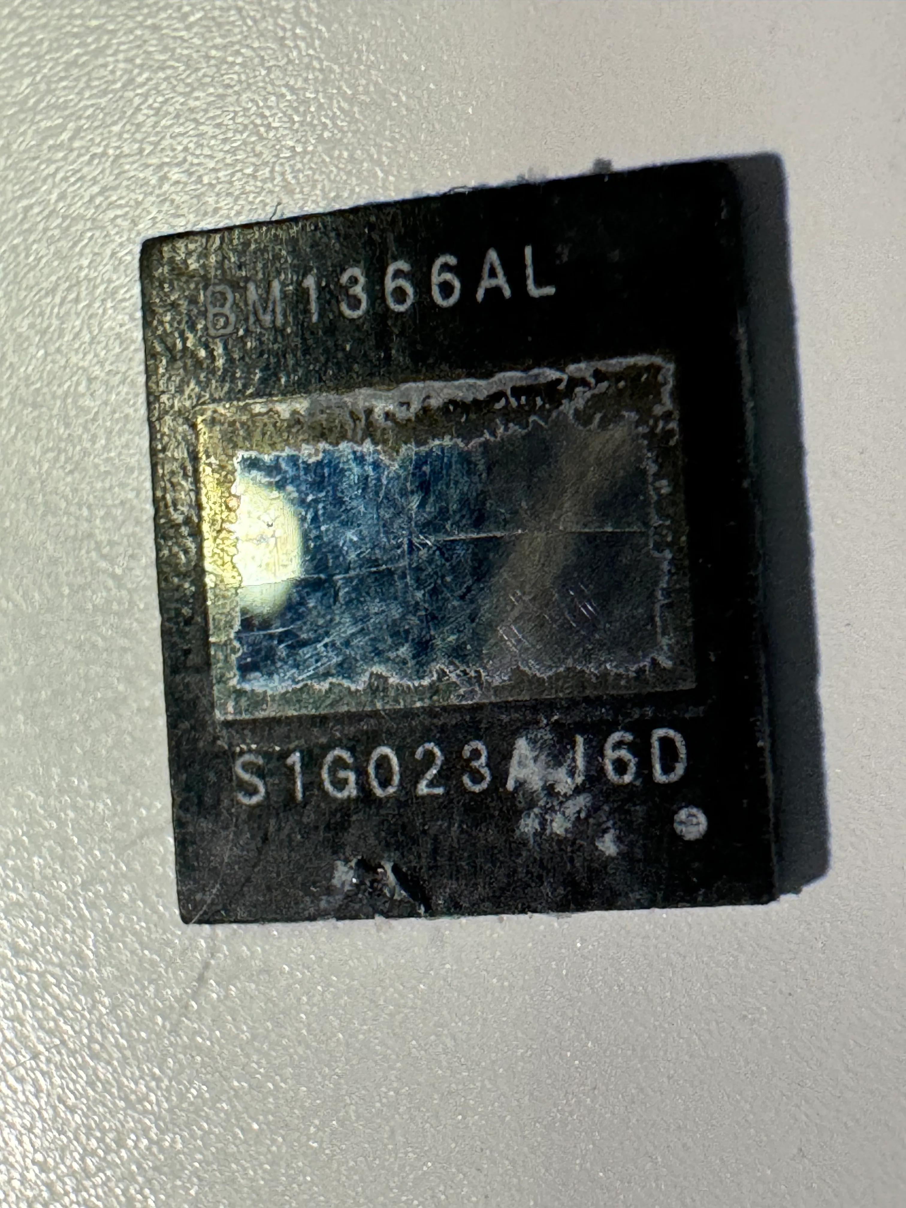
Here you can cleary see a crack right in the middle of the die. This indicates too much heat on the chip itself probably during a soldering attempt. This crack identifies that this chip will no longer work and therefore has been destroyed. It has multiple versions.